P01 1:1 model · not yet built
Digital IC tester
A bench tester for 74xx and 4000-series DIP logic chips: 28 channels, one ZIF socket and an ESP32-S3. ScrollSwipe the cards to take it apart, one layer at a time.
- Status
- Design stage
- Enclosure
- 196 × 126 × 20.9 mm
- Main PCB
- 190 × 120 × 1.6 mm
01 Enclosure
Four screws from below
Four M3×14 socket caps pass up through the corner columns of the base and into heat-set inserts in the lid. Four 12 × 3 mm rubber feet sit under the floor.
- Walls, floor
- 2.5 mm, 2.5 mm
- Base / lid split
- Z 12.0 mm
02 Lid
The lid lifts off
A printed 2.5 mm top that fits over a 1.5 mm alignment lip on the base with 0.1 mm clearance. It prints upside down, top face on the bed. Cutouts let the TFT, the ZIF socket, the keypad tail, a light pipe and the buzzer through.
- TFT window
- 60.5 × 46.2 mm
- ZIF opening
- 67.8 × 32.4 mm
03 Input
Membrane keypad
A 4×4 membrane keypad sticks to the lid. Its 20 mm tail drops through a slot in front of it to a right-angle 1×8 header on the main board.
- Keypad
- 69.2 × 76.9 × 0.8 mm
- Source
- Typical listing, to be measured
04 Device under test
Socket and chip
A 40-pin universal ZIF socket takes 0.3 in and 0.6 in DIPs and stands 5.2 mm above the lid. It plugs into a turned-pin DIP-40 socket on the main board, so a worn one lifts straight out through the lid opening and a spare goes in. Pin 1 goes at the lever end, on the left. The 74LS00 is shown inserted that way.
- Length
- 61.2 mm body, 65.8 with lever
- Width, height
- 25.4, 11.9 mm (typical)
05 Display
2.8 in TFT
An ILI9341 SPI module (MSP2807). Its 14-pin header is soldered into the main board and holds the module in place. Four 2.5 mm nylon spacers carry it and four nylon dowels locate it. The glass ends 0.2 mm under the lid.
- Module PCB
- 86 × 50 × 1.6 mm
- Visible area
- 59.45 × 45.2 mm
06 Main board
The main PCB comes out
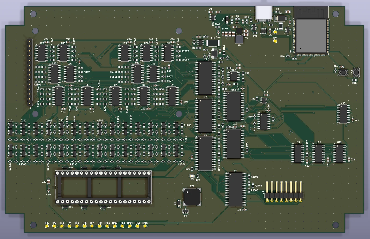
It sits on four 6 mm standoffs. This is the Rev A board from KiCad: four layers, routed, no DRC errors. The 28 channel cells sit in two bands behind the ZIF, each with a high-side and a low-side MOSFET and eight resistors. The shift registers and strong drivers sit under the TFT, where nothing is taller than 2.3 mm, and the four MCP23S17 expanders are to its right.
Not ordered or built yet, and no second person has reviewed the layout.
07 Controller
ESP32-S3 module, on the board
An ESP32-S3-WROOM-1 module is soldered straight to the main board, its antenna end on the back edge. Nothing hangs underneath, so the board sits on 6 mm standoffs and the enclosure is 12 mm lower than with a development board.
- Module
- 18 × 25.5 × 3.1 mm
- Radio
- Not used
08 Back wall
One USB-C port
The only connector. It brings in 5 V and the ESP32-S3’s native USB: console, firmware updates and chip-library uploads. A buck-boost regulator beside it makes the 5 V rail. The receptacle face sits at the inside of the wall, so the opening is sized for the plug’s overmold, not the receptacle.
- Opening
- 13 × 7 mm at X 140
- Receptacle
- 16-pin top mount, typical
09 Assembly
Every part, 1:1
Parts with a datasheet drawing use its sizes. The ZIF width and height, its turned-pin socket, the keypad and the USB-C receptacle are typical values to measure on the real parts. Nothing has been printed or built yet.
One channel, 28 times
Every socket contact gets the same cell, so firmware decides what each pin is. Power and ground can land on any pin: the 7490, for example, has VCC on pin 5. Every pin also goes through a mux to a buffered ADC, so the tester reads voltages and compares them with the TTL or CMOS limits for that chip.
The 470 Ω drive limits the current if a chip output fights it, but the calculations showed that standard-TTL clock inputs pull it too far. So Rev A adds a 110 Ω strong path, which firmware switches on for one pin at a time, and only when that driven-low pin reads between 0.8 V and 2.4 V.
good 7400
  7400 powered, supply current 2.00 mA
  PASS: 7400, 6 checks

7400 with gate 1 stuck low
  line 14: pin 3 (1Y) should be H, reads 0.20 V
  line 15: pin 3 (1Y) should be H, reads 0.20 V
  ...
  FAIL: 7400, 4 of 6 checks failed

7400 inserted backwards
  supply current 250.0 mA is over the 60 mA limit:
check orientation and chip typeWhere it stands
Everything here is a design, a calculation or a simulation. No board has been ordered, no firmware has been flashed and nothing has been measured.
What has been checked
Recorded on 2 November 2026. The library and firmware tests were run again on 5 November.
| Check | Result |
|---|---|
| Schematic ERC, KiCad's own tool | 0 violations |
| KiCad's netlist against the design description, pin for pin | 306 nets, 0 differences |
| Board DRC with schematic parity | 0 errors, 0 unrouted, 18 silkscreen warnings |
| Board model in the enclosure model | 0 overlaps; tallest part under the TFT 1.84 mm of 2.3 mm |
| Firmware tests on a PC, against a register-level model of the board | 116 of 116 pass (simulated) |
| Firmware board map against the Rev A netlist, pin by pin | No differences |
| Production firmware compiled for the ESP32-S3 | Passes; not flashed |
| Chip library checker | 59 files, 0 errors |
What the checks found
- USB inrush. The input capacitors came to about 13 µF after derating, above the 10 µF a USB device may present when plugged in. A soft-start switch and a slower converter start now hold the peak at about 0.4 A (calculated).
- Floating inputs. With the socket empty, the strong drivers' inputs could sit at mid-rail and draw current or oscillate. Each line now has a 330 kΩ pull-down.
- The ADC's blind spot. The ESP32-S3's ADC reads 0 for anything below its zero, which left 37 mV of error near 0 V in simulation, against a 30 mV target. A factory load board now gives a second calibration point, which brings it to 2.1 mV in simulation.
- A slow fight check. A chip output fighting the strong path was caught after 198 µs, at the edge of the 200 µs target. A shorter check does it in 73 µs, also simulated.
Not done yet
- The four-channel breadboard prototype, and any bench measurement.
- The fabricator's design check on the Rev A board, a real quote and the order.
- Flashing the firmware. The display, keypad, storage and real timings have never run on a board.
- Running the chip library on real chips, and a second reader for the newest 37 of the 59 files.
- Printing the enclosure and fit-testing it on real parts.
Next
Build the four-channel prototype on a breadboard, run the empty-socket self-test and then a known-good 74LS00, and record the real supply current and output voltages. Those measurements replace the design's assumptions and decide whether Rev A goes to fabrication as it stands.
Open the model
The model is parametric: every dimension is a named constant, so changing one and rebuilding updates every part. It is a design, not a measured prototype. The main board in it is the routed Rev A board from KiCad. Nothing has been printed or tested yet.
- Interactive modelOrbit, orthographic views, explode, section cut and measure, in the browser
- ic-tester-assembly.glbThe full assembly as glTF (10.6 MB), for Blender or any web viewer
About the IC tester
What chips does the IC tester test?
74xx and 4000-series logic chips in DIP packages. A 40-pin universal ZIF socket takes both 0.3 in and 0.6 in wide DIPs, and the tester has 28 channels.
Has the IC tester been built?
Not yet. It is in the design stage. The Rev A schematic and four-layer board are routed and pass KiCad's electrical and design rule checks, and the firmware passes its tests in simulation. No board has been ordered, no firmware has been flashed, and nothing has been printed, built or measured.
What does it report when a chip fails?
It is designed to name the failing pin, the gate it belongs to, the level it expected and the voltage it measured. A chip inserted backwards trips a current limit, and the tester switches its supply off before reporting it.
How many chips can it test?
The library has 59 chip files: 47 for 74xx parts and 12 for 4000-series parts. Each one is a plain text file, so adding a chip needs no new firmware. None has been run on a real chip yet.
What is inside the IC tester?
An ESP32-S3-WROOM-1 module soldered to the main board, four MCP23S17 I/O expanders, eleven 74HCT595 shift registers, seven 74ACT125 strong drivers, two CD74HCT4067 sense muxes and 28 channel cells, each with a high-side and a low-side MOSFET and eight resistors. A 2.8 in ILI9341 SPI TFT sits on the main board and a 4×4 membrane keypad sits on the lid.
How big is the IC tester?
The enclosure is 196 × 126 × 20.9 mm, or 23.9 mm tall on its rubber feet. The main PCB is 190 × 120 × 1.6 mm.
How is the IC tester powered and connected?
Through one USB-C port in the back wall. It brings in 5 V and the ESP32-S3 native USB, for the console and firmware updates, and a buck-boost regulator beside it makes the 5 V rail for the board.
Can I download the IC tester 3D model?
Yes. Open the interactive model to orbit, explode, section and measure it in the browser, or download the full assembly as a 10.6 MB glTF file, ic-tester-assembly.glb, for Blender or any web viewer.